Angstrom process
control for the AI era.

Infinitesima develops the metrology technology enabling
the next generation of semiconductor manufacturing.

Infinitesima develops the metrology technology enabling the next generation of semiconductor manufacturing.

The industry is changing

As semiconductor manufacturing reaches unprecedented levels of complexity, three fundamental challenges are pushing conventional metrology beyond its limits and redefining what process control requires.

As semiconductor manufacturing reaches unprecedented levels of complexity, three fundamental challenges are pushing conventional metrology beyond its limits and redefining what process control requires.

Advanced Packaging

Icon

Hybrid bonding demands angstrom-scale process control.

Advanced Packaging

Icon

Hybrid bonding demands angstrom-scale process control.

Complex 3D Devices

Icon

Next-generation architectures require true 3-dimensional measurement.

Complex 3D Devices

Icon

Next-generation architectures require true 3-dimensional measurement.

High-NA EUV

Icon

Shrinking nodes are testing the limits of conventional metrology.

High-NA EUV

Icon

Shrinking nodes are testing the limits of conventional metrology.

The industry is scaling down.

Wafer Scale
Wafer Icon

Continued Scaling
High-NA EUV

And building up.
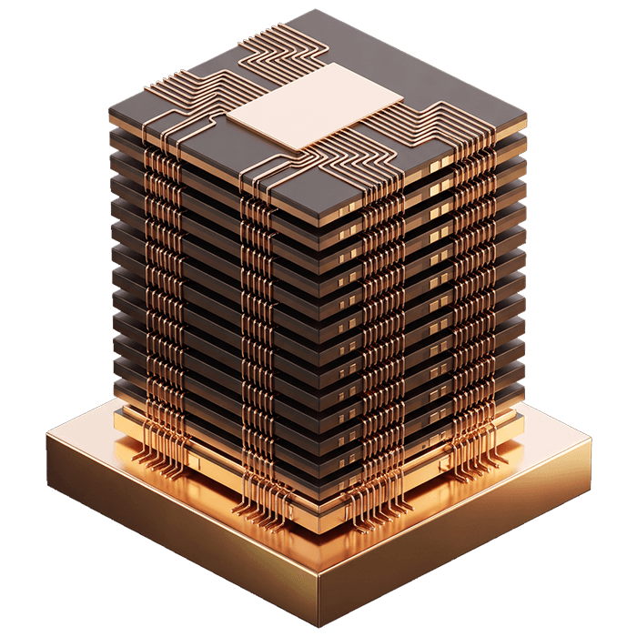
Chip Stack
Chip Icon

Advanced Packaging
& Heterogeneous Integration

Wafer 3D Render

The Gap

The metrology gap requirement is increasing.

The metrology gap requirement is increasing.

Metrology Gap Chart

Customer Impact

Purpose-built for advanced processes.

Probe tip
Better Process Control

Angstrom precision.

True 3D information.

Production speed.

Surface Map
Deeper Understanding

Faster learning cycles.

Catch variation early.

Understand in 3D.

Wafer 3D Render
Tighter Control

Smarter decisions.

Real-time adjustments.

Stable processes.

Chip Stack
Improved Yield

Reduced cost.

Faster time to market.

Consistent quality.

Why it matters

Technologies that shape tomorrow.

Technologies that shape tomorrow.

Tomorrow's technologies depend on semiconductors manufactured with unprecedented precision. Infinitesima provides the process understanding required to manufacture them with confidence.

Tomorrow's technologies depend on semiconductors manufactured with unprecedented precision. Infinitesima provides the process understanding required to manufacture them with confidence.

Application Illustration
Metron3D

Our Product

Probe tip.

Metron3D combines angstrom-scale measurement with production throughput, delivering capabilities no alternative metrology platform can match.

Explore features by hovering

Metron3D

Our Product

Probe tip.

Metron3D combines angstrom-scale measurement with production throughput, delivering capabilities no alternative metrology platform can match.

Explore features by hovering

Product Specs

01

Fully automated 300 mm wafer handling, dual-arm robot.

02

SECS / GEM factory automation integration.

03

Modular architecture for reliability & uptime.

04

Automated probe handling with integrated health-check.

05

Fast optical pattern recognition & wafer alignment.

Trusted across the semiconductor ecosystem.

Trusted across the
semiconductor ecosystem.

Infinitesima works alongside leading semiconductor manufacturers, research institutes and technology partners to solve some of the industry's most demanding metrology challenges.

  • Innovation Network

    Imec
  • Innovation Network

    University of Sheffield
  • Sales Network

    MIC
  • Innovation Network

    NPL
  • Innovation Network

    University of Bristol
  • Sales Network

    Woowon Technology
  • Sales Network

    Canon Marketing Japan
  • Innovation Network

    Imec
  • Innovation Network

    University of Sheffield
  • Sales Network

    MIC
  • Innovation Network

    NPL
  • Innovation Network

    University of Bristol
  • Sales Network

    Woowon Technology
  • Sales Network

    Canon Marketing Japan
  • Innovation Network

    Imec
  • Innovation Network

    University of Sheffield
  • Sales Network

    MIC
  • Innovation Network

    NPL
  • Innovation Network

    University of Bristol
  • Sales Network

    Woowon Technology
  • Sales Network

    Canon Marketing Japan
Metron3D Arm

Performance backed by proof.

Performance backed
by proof.

Patent Families

40+

Years of research

25+

Production Validation

Lowest Cost Per Wafer

AFM Precision at Speed

True 3D Profile

“Three-dimensional process control at the nano-scale level is becoming increasingly important to ensure high yield in advanced DRAM processes. Infinitesima's Metron3D has demonstrated excellent sub-nanometre 3D metrology with the required cost-of-ownership necessary for HVM implementation.”

SK hynix

Young-Hyun Choi, Head of DMI, SK hynix

"Scaling now requires true 3D process control at atomic scale. We are enabling this by delivering revolutionary high-speed, ground-truth 3D surface metrology with atomic resolution – capabilities that are increasingly essential for next-generation devices."

Infinitesima

Prof. Andrew Humphris, Founder & CTO, Infinitesima

Metron3D Close up