
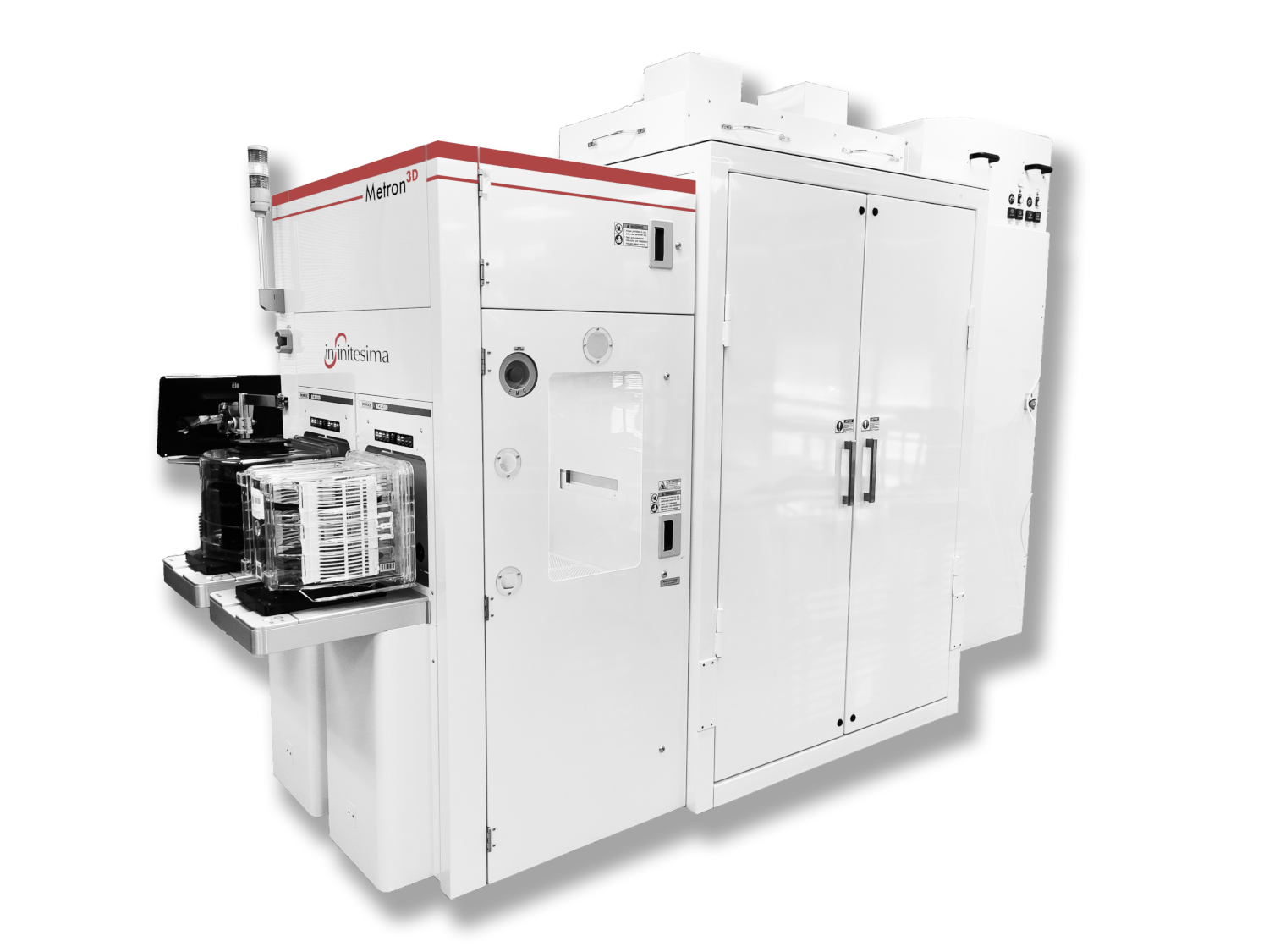
Infinitesima have completed the first customer shipment of the Metron3D metrology system, a revolutionary sub-nanometer, high speed 3D imaging system that operates at in-line production throughputs.The system has passed all internal qualification tests for imaging quality and throughput and is being shipped to an undisclosed, leading Semiconductor manufacturer. With imaging time measured in seconds, rather than minutes the system will address metrology challenges for manufacturing next generation logic, DRAM and 3D NAND devices.
The Metron3D has demonstrated throughput and imaging speeds up to 100x faster than conventional atomic force microscopy (AFM) technology, achieved through a patented photo-thermal actuation of the probe tip. Fully automated for high throughput in-line operation, the system features a wide field of view optical global align system, high-speed wafer stage, and a probe library with fully automated probe exchange. To ensure imaging quality in a manufacturing fab environment, the system has been designed to withstand acoustic noise and vibration through resonance modelling and multi-layer acoustic isolation.
Metrology is essential to maximise the yield, and hence cost efficiency of Semiconductor fabrication. Technology inflections towards High NA EUV, hybrid wafer bonding, and complex 3D device structures are now moving beyond the capability of existing e-beam and optical techniques and are a limiting factor for further progress.
A key example is the coming transition to High-NA EUV, where smaller features require higher resolution metrology, but the thinner resists reduce image contrast and are more sensitive to damage when using e-beam techniques. Probe metrology is well established as a lab technique and has the resolution and 3D imaging capability to overcome these challenges but has traditionally been too slow for in-line integration. The Metron3D breaks this paradigm, providing probe metrology at the high throughput necessary for in-line process control.
Reflecting on the challenges for next generation devices John Cossins, Marketing and Business Development Director comments that “this is a pivotal moment, not just for Infinitesima, but for the wider Semiconductor Industry, bringing a new technique to in-line manufacturing. We fully expect this to be the beginning of a broad adoption of probe metrology as existing techniques reach their limits”.
Further developments are underway and Andrew Humphris, CTO has his eyes on the future of the technology. “The team are extremely proud to have delivered this capability, and the performance of the tool has exceeded expectations. Now we are excited to be looking to the next innovations on the roadmap as we work towards a further order of magnitude improvement in imaging speed.”