
In semiconductor manufacturing, the RPM can be applied to both Metrology or Inspection applications. In addition, the RPM offers some unique capabilities that are well suited to solving problems in the research lab, examples of each are given below.
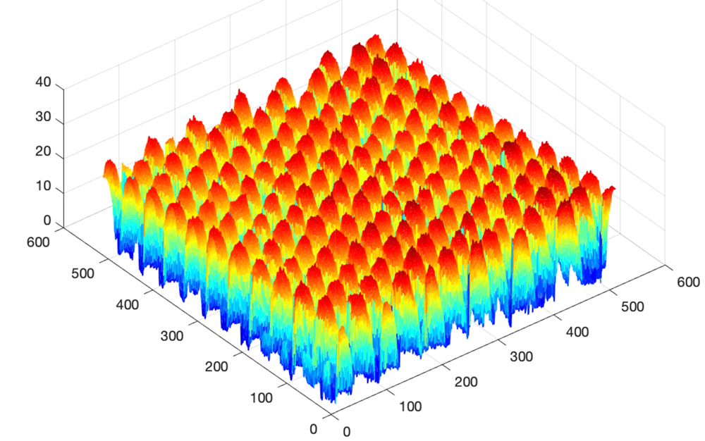
Metrology applications are focused on specific measurements of structures and defects. This can include measuring both the lateral and vertical critical dimensions of a structure, measuring the roughness of a surface, or measuring the flatness of a surface over a specified area.
Inspection applications typically involve looking for defects or abnormalities in surfaces or patterns over larger sample areas.
R&D is focused on developing process and methods for future manufacturing. The RPM can be applied to characterise devices and process during development. Material properties can be determined using different RPM drive modes.
Lithography or ‘Litho’ is the process of transferring the device pattern from a mask (template) into a photo-sensitive film on the wafer called photoresist or simply ‘resist’.
The latest generation of Litho processing, termed EUV, uses a wavelength of 13.5nm which can currently pattern features down to a pitch of 26nm. A future extension of this technology with higher numerical apertures: High NA EUV, will extend this to a pitch of 16nm.
EUV and high NA require a very thin resist layer, which are difficult to image with optical and e-beam metrology techniques, due to limited contrast. In addition, these thin layers are very sensitive to damage and a resulting change in size (shrinkage) when exposed during measurement by these techniques.
However, the capability to measure EUV patterns is critical. Due to the energy of EUV photons, operation at low exposure doses, and the nature of the resist chemical interactions, EUV Litho processes exhibits a high level of Stochastical variation. Measuring and monitoring this variation is key to controlling the process and yield.
The RPM can measure both the lateral and height of EUV resist within the actual device. This is achieved without damaging the resist and is therefore an ideal solution for EUV litho metrology. Furthermore, the RPM can measure any stochastic variation in the resist pattern and find stochastic defects.
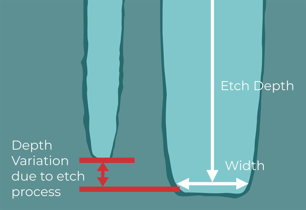
Etching is the process of transferring the Litho pattern into the wafer by selectively removing those areas not protected by the resist. The etch process used for advanced semiconductors is usually plasma or reactive ion etching.
The rate that material is removed or ‘etched’ from the wafer can differ across the wafer due to variations in the gas flow, it can also vary within a device due to differences in the size of features and pattern density.
It is critical in etching processes to ensure that the correct depth is achieved to guarantee correct device functionality. Under etching can result in device failure, over etching can damage or remove the underlying film causing device performance issues or failure. Therefore, metrology techniques which can accurately and reliably measure depth on the nano scale are required.
E-beam techniques do not accurately measure structure depth and optical metrology is constrained to measuring large targets outside of the device, so cannot detect local variation in etch depth e.g. from pattern loading effects.
In this application, the RPM delivers benefits which these other tools cannot. Etch depth is measured with an accuracy typically of 0.5nm 3 sigma, over a wide range of etch depths and feature sizes. This then enables the etch process to be both optimised and controlled effectively.
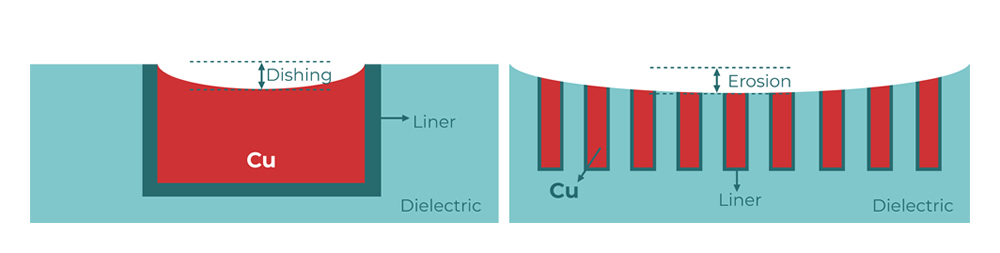
Chemical-Mechanical Polishing, CMP, as its name implies involves the combination of chemical and mechanical interactions to polish the surface of the wafer. This planarization occurs after the deposition of films over a patterned structure and is required to prepare the surface prior to the next step in the device fabrication process.
CMP is an increasingly critical step in advanced chip processes. This s driven by the move to complex 3D structures coupled with the very small depth of focus available with EUV and High NA EUV. This requires the planarisation of the chip across the wafer to be consistently within a few 10s of nano-meters. The uniformity of the polishing can be influenced by the pattern density which can result in yield limiting ‘hot spots’ within the chip.
Measuring the planarisation has typically required optical systems, either using white light interferometry which can be sensitive to thin film interference effects or Scatterometry which requires special targets that lack information on within chip pattern effects.
The RPM is ideally suited to this application as it can measure high speed intra-die polishing uniformity and flatness metrology to < 0.5nm 3 sigma.
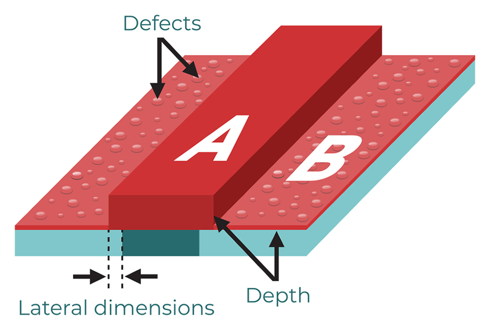
Thin film deposition processes deposit a wide range of materials in the chip fabrication process and can involve a variety of different techniques. The most common are chemical vapour deposition, CVD, physical vapour deposition, PVD, epitaxial deposition, and more recently, atomic Layer deposition, ALD. New techniques, such as selective deposition, where the film is only deposited on certain areas of the device, and the deposition of new materials, such as Ruthenium are important for future devices.
A variety of metrology techniques are used to measure a deposited films properties, including film thickness and uniformity, step coverage, surface roughness, film composition, and defect density.
As these films have become thinner, and the topography on which the thin film is deposited more complex it has become increasingly difficult for optical and e-beam techniques to provide the required metrology information. The ability of the RPM to detect small defects, measure the grain size of deposited metals and the change in step height resulting from selective deposition make it a valuable addition in the development and characterisation of new deposition processes. As these processes are introduced into production for future generation devices, the RPM can enable in-line defect monitoring..
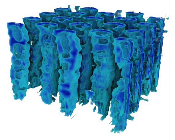
As advanced Semiconductor devices become increasingly complex in the 3rd-dimension, there is increasingly the need to be able to measure and inspect a vertical cross section through the device.
This can currently be achieved, using either a cross-section scanning electron microscope or a transmission electron microscope. Here a Focused Ion Beam, FIB, system is typically used to create the device cross section. In the case of TEM, additional steps are needed to create an electron transparent, lamella of the device. This sample preparation is both time consuming, expensive, and may be coupled with added complication of damaging ions being implanted into the sample surface.
The RPM can perform 3D tomography in-situ on the wafer, by application of a hard probe for atomic layer removal, ALR, and a bespoke probe for either height measurement of current measurement. This switching between probes is automated with a co-localised positioning of the probes for efficiency and ease of use. As a result a sequence of steps; ALR followed by measurement enable a 3D tomographic cross section of the device to be produced. The automated nature of this process means a 3D section can be achieved in minutes rather than hours, the result is fast cycle times without the need to scrap the wafer.
Infinitesima Limited
Suite 1, Hitching Court, Abingdon Business Park, Abingdon, Oxfordshire, OX14 1RG, United Kingdom
Telephone: +44 (0)1235 525922
Email: info@infinitesima.com